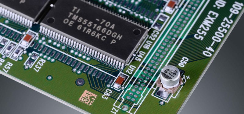
Printed circuit boards are used in almost every category of electronic product and are often described as a foundation of electronic systems. Rising PCB quality requirements have increased the need to manage production and quality information. Marked characters, barcodes and two-dimensional codes provide a practical basis for that traceability.
The two main marking approaches discussed here are screen printing and laser marking.
In conventional screen printing, a prepared mesh stencil transfers ink to the board under pressure. Open parts of the mesh form the lettering, identifiers or graphics, while blocked areas remain unprinted. The process is comparatively inexpensive and fast, but markings can be coarse or detach, very small boards are difficult to mark, and chemical inputs introduce additional handling considerations.
Laser marking directs a high-energy-density beam onto a local PCB area, vaporising or changing the colour of the surface material to leave a persistent mark. The non-contact process can create clear two-dimensional codes in small areas with high positional precision. The described benefits include resistance to temperature changes, chemical exposure and abrasion, while avoiding auxiliary marking chemicals.
Dedicated PCB laser marking equipment offers precision and flexibility that address limitations of screen printing. It can improve production efficiency and yield while reducing marking costs and chemical inputs. Applications include digital products, wearable devices and automotive circuit boards.